- MEMRISTORS AND MEMRISTIVE SYSTEMS
After the first introductions of memristors and memristive systems in 1971 and 1976 by Leon Chua and Steve Kang, researchers in HP Lab reported a successful physical realization and understanding of memristors and its switching mechanism in 2008, opening world-wide research efforts related to memristors. Potential applications include nonvolatile resistive memories, memristor-based ultra high density Boolean logic gates without active transistors, neuromorphic applications to simulate learning, adaptive and spontaneous behaviors.
Our research group is working on memristors and memristive systems, in particular the following areas.
(a) Compact modeling of memristors
Recently our group introduced compact models for memristors [TCAD-2010]. Unlike the previously reported other memristor modeling methods, our approach is uniquely based on the constitutive relationship of memristors between charge and flux. Since a memristor provides a unique constitutive relationship by its definition, our modeling method can be applied to any memristor device, regardless of whether it possesses its physical equations or not, and the model parameters can be easily extracted from measured constitutive relationships.
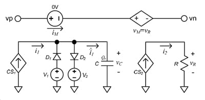
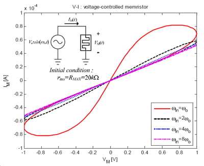
The modeling process with a few simple steps was also developed. Especially for practical memristors with limited resistance ranges, a simple method to find their constitutive relationships was discussed, and examples of compact models were shown for both current-controlled and voltage-controlled memristors. Our models satisfy all of the memristor properties such as frequency dependent hysteresis behaviors and also unique boundary assurance to simulate memristors whether they behave memristively or resistively. Our models are implementable in circuit simulators, including SPICE, Verilog-A, and Spectre.
– link to spectre model
(b) Memristor applications for programmable analog ICs
Since a memristor should be able to change its resistance very finely by controlling its excitation history, it would provide programmable resistance without any use of switch device that can have impact on a broad range of electronics in which fuse/anti-fuse or switch based electrical trimming circuits, variable RC delay lines, and many others can be replaced with compact memristor-based circuits. We are putting our effort to create new memristive circuits whose performance can be superior to the state-of-the-art conventional circuits. Proper biasing and read/write circuits are being investigated to implement new functions.
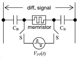
As an example of utilizing memristors to compensate for existing limitations of CMOS circuits, we have demonstrated that memristors can be used to implement programmable analog circuits, leveraging memristor’s fine resolution programmable resistance without causing perturbations due to parasitic components [TNANO-2010]. Fine resolution programmable resistance is achieved by varying the amount of flux across memristors. We have shown that the resistance programming can be achieved by controlling the input pulse width and its frequency. In particular, we have introduced a pulse-controlled memristor as a demonstrative example of input patterning, and a programmable gain amplifier for circuit application, which aim to provide details on analog IC applications for which unique properties of memristors are properly used and controlled.
The application can be extended to amplitude modulators, RF-DACs, and others.
(c) Non-volatile resistive memory
Toward this application, memristors are considered a most promising candidate due to their great potential for inexpensive manufacturing together with ultra high density. Since memristive devices can be formed in simple thin-film devices, they are compatible with CMOS processes. The basic structure for a memory and most other applications is a simple crossbar structure, which can be easily fabricated with very high area density. A passive memory array, such as a passive R-RAM, that does not require devices for cell selection will yield much higher area density and very low readout power consumption.
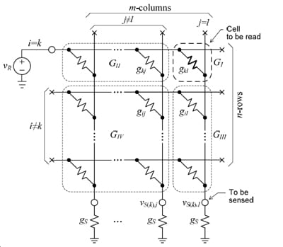
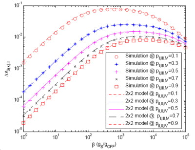
It is known that the detection margin of a passive R-RAM is highly dependent on distributions of stored data. While a worst case circuit model regarding the data pattern has been reported in 1969 [Lynch,TC-1969], our group introduced a 2×2 equivalent statistical memory model dealing with sneak currents and random data distributions for nxm passive memory arrays of memristive devices. The data-dependent 2×2 circuit model enables a broad range of analyses, such as the optimum detection voltage margin, with computational efficiency and has no limit on the memory array size. Also, we proposed replica-based self-adaptable sense resistors to achieve both low-power reading and large voltage detection windowing.
(d) Memristive signal processing
It is much desirable that for many systems the system configuration is self-adaptable to the environments or to the input or sensed signal quality. Such systems include biological and medical diagnosis, distributed sensor nodes, chemical environment monitoring, smart power control, multi-mode multi-standard communication systems, etc. It is expected that the memristors and/or memristive devices provide an efficient way of system adaptation and re-configurability when their memory and learning properties are properly understood. Among many of potential applications of memristors, we are exploring a low-power memristive signal processing unit that can estimate and analyze the signal quality and statistics by properly controlling the memristive circuit signals.
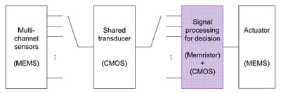
Our special long-term research is aimed to build memristor-based complete standalone reconfigurable systems, while the short term goal is to develop monitoring and signaling methods that can be easily extended to the other applications. Related research is expected to show a clear direction toward how a group of memristive devices can monitor and process signals. Successful completion of this research can greatly impact many areas of electronics, in particular the distributed sensor networks, biomedical diagnosis, and environmental monitoring systems, by providing practically applicable signal monitoring and decision making for system adaptation.
(e) Design automation for hybrid integration of memristive devices and CMOS circuits
A hybrid type of memristors/CMOS integration is a promising technology toward the future low-power and high density integrated circuits. Our group is conducting special research activities toward the high-level automation for the hybrid system integrations, from the memristive logic synthesis to automated placement and route.
In addition, the memristive devices are explored, by harnessing their non-volatility, for many other analog/digital circuits that require switching or data storage, such as flip-flops, FPGA, etc.
(f) Memristor-inspired wireless chaotic communications
Memristor circuits are also known to provide quasi chaotic signals that can be directly used to compose chaotic communications. Many researchers reported on memristor circuits’ potentials for coherent or non-coherent chaotic communications by properly utilizing the memristive chaotic signals.
We are investigating a MIMO implementation of wireless chaotic communication systems in particular for non-coherent ultra wideband applications. The MIMO extension, together with the randomness and wideband features of the memristive chaotic signals, can provide much superior diversity performance and higher throughput over the widely considered SISO systems. The MIMO system would be best fit for indoor high throughput wireless applications, such as wireless HDTV or USB.
- LOW-VOLTAGE HIGH-SPEED VLSI CIRCUITS
As the CMOS technology scales down, traditional analog/RF circuit design methodologies are also evolving by exploiting innovative circuit techniques such as low-voltage and sub-threshold circuits, and all digital implementations. Nano-scale CMOS technology offers a potential for small size, high integrity, fast switching speed with finer timing resolution. However, the demand for low power consumption requires that the supply voltage scaling be lowered much faster than the threshold voltage scaling, and thus resulting in the tough voltage headroom problem, especially for the analog/RF circuit designers.
The small headroom causes limited voltage resolutions and thus poor linearity performance. Moreover, along with low output impedance, the deep submicron devices show much poor noise performance since the short channel devices usually generates much higher 1/f noise than the long channel devices, implying that it will be very difficult to achieve wide enough dynamic range offering acceptable signal-to-noise performance. Whereas the downward scaling challenges greatly analog/RF circuit designs, it provides advantages for digital circuits. Current CMOS technology offers cutoff frequencies of up to several hundred GHz, and thus the high speed direct digital implementation even for the GHz range RF signals can be an alternative to get over the limited headroom and linearity problems.
Our group is actively pursuing development of next generation analog/RF circuit techniques exploiting as many digital techniques as possible, eventually for the true Software Defined Radio (SDR) with flexible configurability, which can be easily integrated on a chip together with many types of applications.
Together with high-speed circuit techniques such as GHz range data converters and all-digital frequency synthesizer, our research includes the systematic architectural study to preserve the analog-like high precision and low-noise digital performance, and multi-level high speed bi-directional input/output circuits.
(a) High resolution data converter
Recently, high-speed and high-accuracy digital-to-analog converters (DACs) have been widely applied to HDTV, video, and modern communication systems. While designing DACs, the important design issues of interest are how to integrate analog circuits together with digital switching circuits on the same chip regarding SOC integrations. In addition, static performance parameters such as offset error, gain error, INL, DNL are also of our interest.
While the static performances of current steering DACs are limited by the random error and systematic error, the dynamic performances are typically limited by three factors: 1) voltage fluctuation in the output nodes due to improper timing; 2) control signal feed-through to the output lines; and 3) imperfect synchronization of the switching signals. In order to achieve high performance, a statistical systematic analysis dealing with the parameter mismatch, transistor gate area, cell switching sequences, and PVT variations are considered.
Along with the systemic analysis and circuit design, we are developing an accurate mathematical model for the transistor size effects and PVT variations to provide an explicit way of performance optimization regarding conversion resolution, linearity, and dynamic performances of SFDR and SNDR.
(b) Multi-level simultaneous bi-directional high-speed I/O
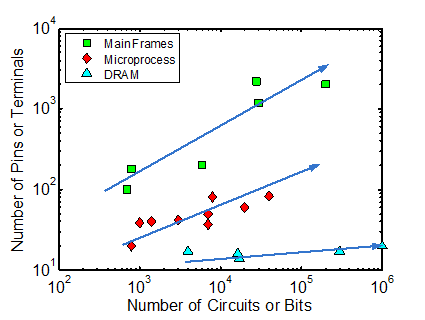
To accommodate the VLSI trend of rapid increase in circuit size, geometries are being aggressively scaled down. This downscale increases the need to communicate with the external system such as storage, display, or any further data processing. Also, the longer word size and the higher data rate in the chip interface lead to increase in the number of I/O pins in a unit area of a package and the power dissipation as well.
In chip-to-chip communications, the topology of the communications affects the performance of the communication links. Multi-drop is a configuration in which components are all connected to the same set of communication wires. It polls data in sequence over one communication wire that results in a cheaper solution at the expense of response time.
Point-to-point dedicates one communication line between two chips. It is usually preferred for the high speed links that require high reliability even though it comes with large number of I/O. In a point-to-point link, increasing the bandwidth per wire enhances system performance due to limited number of pins. Simultaneous Bidirectional (SBD) signaling was previously introduced to allow simultaneous data transmission in two directions over one wire, doubling the effective bandwidth per pin over a point-to-point unidirectional transmission. The multi-level SBD I/O enhances data rate over SBD I/O at the expense of less voltage distance.
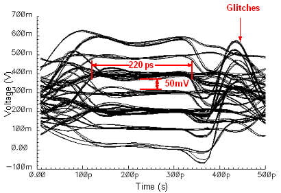
This research is to develop a reliable high speed multi-level simultaneous bi-directional I/O. When an I/O switches data at high speed, it draws a large current abruptly to drive output loads, which causes simultaneous switching noise (SSN) induced by parasitics. A differential scheme is one of the best solutions that make the total sum of AC currents ideally zero. To increase data rate, firstly calibration is considered for the impedance mismatch between the two chips which reduces the voltage margin and for the mismatch between voltage references and incoming signal which degrades Symbol Error Rate (SER). Also, a band-gap reference is used to reduce the effects of supply voltage fluctuation, temperature variation, and chip-to-chip mismatches. Secondly, in an I/O, a large size of current switches limits the bandwidth. A latched differential current switching scheme and pre-emphasis enhance speed in the transmitter. In the receiver end, de-emphasis to a voltage references and a clocked comparator are applied for the higher symbol rate. Simulation based on 0.18um CMOS process show that the proposed design achieves data rate up to 8-Gb/s/pin at the power consumption of 46.8mW with 1.8V power supply. A test chip is developed for experimental verification.